Graphene, an emerging material that could change the way electronic components are made and help computing performance continue to grow, is everywhere in the research world these days.
This month alone, advancements suggested it could boost internet speeds, serve as a touch sensitive coating and extend the lives of computers. It is stronger than diamond and conducts electricity and heat better than any material ever discovered, and it will likely play an important role in many products and processes in the future.
What is graphene?

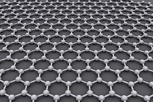
Graphene is made of a single layer of carbon atoms that are bonded together in a repeating pattern of hexagons. Graphene is one million times thinner than paper; so thin that it is actually considered two dimensional.
Carbon is an incredibly versatile element. Depending on how atoms are arranged, it can produce hard diamonds or soft graphite. Graphene’s flat honeycomb pattern grants it many unusual characteristics, including the status of strongest material in the world. Columbia University mechanical engineering professor James Hone once said it is “so strong it would take an elephant, balanced on a pencil, to break through a sheet of graphene the thickness of Saran Wrap,” according to the university.
These single layers of carbon atoms provide the foundation for other important materials. Graphite — or pencil lead– is formed when you stack graphene. Carbon nanotubes, which are another emerging material, are made of rolled graphene. These are used in bikes, tennis rackets and even living tissue engineering.
How was it discovered?
Chances are good that you have made graphene many times in your life. Draw a line with a pencil and small bits of graphene will flake off. But no one had both the tools and interest to reliably isolate free-standing graphene until the early 2000s.
Graphene was first studied theoretically in the 1940s. At the time, scientists thought it was physically impossible for a two dimensional material to exist, so they did not pursue isolating graphene. Decades later, interest picked up and researchers began dreaming up techniques to peel apart graphite. They tried wedging molecules between layers of graphene and scraping and rubbing graphite, but they never got to a single layer. Eventually, they were able to isolate graphene on top of other materials, but not on its own.
In 2002, University of Manchester researcher Andrew Geim became interested in graphene and challenged a PhD student to polish a hunk of graphite to as few layers as possible. The student was able to reach 1,000 layers, but could not hit Geim’s goal of 10 to 100 layers. Geim tried a different approach: tape. He applied it to graphite and peeled it away to create flakes of layered graphene. More tape peels created thinner and thinner layers, until he had a piece of graphene 10 layers thick.
Geim’s team worked at refining their technique and eventually produced a single layer of carbon atoms. They published their findings in “Science” in October 2004. Geim and his colleague Kostya Novoselov received the Nobel Prize in physics in 2010 for their work.
Since those first flakes made with tape, graphene production has improved at a rapid pace. In 2009, researchers were able to create a film of graphene that measured 30 inches across.
Why is it unusual?
Geim and Novoselov’s paper was wildly interesting to other scientists because of its description of graphene’s strange physical properties. Electrons move through graphene incredibly fast and begin to exhibit behaviors as if they were massless, mimicking the physics that governs particles at super small scales.
“That kind of interaction inside a solid, so far as anyone knows, is unique to graphene,” wrote Geim and another famous graphene researcher, Philip Kim, in a 2008 Scientific American article. “Thanks to this novel material from a pencil, relativistic quantum mechanics is no longer confined to cosmology or high-energy physics; it has now entered the laboratory.”
Graphene’s special properties don’t stop with weird physics. It’s also:
- Conductive: Electrons are the particles that make up electricity. So when graphene allows electrons to move quickly, it is allowing electricity to move quickly. It is known to move electrons 200 times faster than silicon because they travel with such little interruption. It is also an excellent heat conductor. Graphene is conductive independent of temperature and works normally at room temperature.
- Strong: As mentioned earlier, it would take an elephant with excellent balance to break through a sheet of graphene. It is very strong due to its unbroken pattern and the strong bonds between the carbon atoms. Even when patches of graphene are stitched together, it remains the strongest material out there.
- Flexible: Those strong bonds between graphene’s carbon atoms are also very flexible. They can be twisted, pulled and curved to a certain extent without breaking, which means graphene is bendable and stretchable.
- Transparent: Graphene absorbs 2.3 percent of the visible light that hits it, which means you can see through it without having to deal with any glare.
What can it be used for?
The use of graphene in everyday life is not far off, due in part to existing research into carbon nanotubes — the rolled, cylindrical version of graphene. The tubes were popularized by a 1991 paper (subscription required) and touted for their incredible physical qualities, most of which are very similar to graphene. But it is easier to produce large sheets of graphene and it can be made in a similar way to silicon. Many of the current and planned applications for carbon nanotubes are now being adapted to graphene.
Some of the biggest emerging applications are:
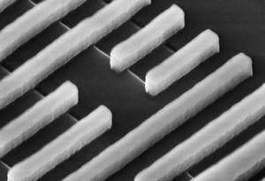
- Solar cells: Solar cells rely on semiconductors to absorb sunlight. Semiconductors are made of an element like silicon and have two layers of electrons. At one layer, the electrons are calm and stay by the semiconductor’s side. At the other layer, the electrons can move about freely, forming a flow of electricity. Solar cells work by transferring the energy from light particles to the calm electrons, which become excited and jump to the free-flowing layer, creating more electricity. Graphene’s layers of electrons actually overlap, meaning less light energy is needed to get the electrons to jump between layers. In the future, that property could give rise to very efficient solar cells. Using graphene would also allow cells that are hundreds of thousands of times thinner and lighter than those that rely on silicon.Intel’s transistors at 32 nanometers. More transistors helped pave the way for cheaper computing.

- Transistors: Computer chips rely on billions of transistors to control the flow of electricity in their circuits. Research has mostly focused on making chips more powerful by packing in more transistors, and graphene could certainly give rise to the thinnest transistors yet. But transistors can also be made more powerful by speeding the flow of electrons — the particles that make up electricity. As science approaches the limit for how small transistors can be, graphene could push the limit back by both moving electrons faster and reducing their size to a few atoms or less.
- Transparent screens: Devices such as plasma TVs and phones are commonly coated with a material called indium tin oxide. Manufacturers are actively seeking alternatives that could cut costs and provide better conductivity, flexibility and transparency. Graphene is an emerging option. It is non-reflective and appears very transparent. Its conductivity also qualifies it as a coating to create touchscreen devices. Because graphene is both strong and thin, it can bend without breaking, making it a good match for the bendable electronics that will soon hit the market.
Graphene could also have applications for camera sensors, DNA sequencing, gas sensing, material strengthening, water desalination and beyond.
What are the critiques?
Graphene is still in an infantile stage compared to developed materials like silicon and ITO. In order for it to be widely adopted, it will need to be produceable in large quantities at costs equal to or lower than existing materials. Emerging roll-to-roll, vapor deposit and other production techniques hint that this is possible, but they’re not yet ready to bring graphene to every mobile device screen out there. Researchers will also need to continue to work at improving graphene’s transparency and conductivity in its commercial form.

Roll-to-roll manufacturing could allow graphene to be made at large scales. Korea University
While graphene shows promise for transistors, it has a major problem: It can’t switch the flow of electricity “off” like materials such as silicon, which means the electricity will flow constantly. That means graphene can’t serve as a transistor on its own. Researchers are now exploring ways to adjust it and combine it with other materials to overcome this limitation. One technique involves placing a layer of boron nitride–another one-atom-thick material–between two layers of graphene. The resulting transistor can be switched on and off, but the electrons’ speed is slowed somewhat. Another technique involves introducing impurities into graphene.
Graphene may also be emerging too late for many of its possible applications. Electric car batteries and carbon fiber could be made with graphene, but they already rely on activated carbon and graphite, respectively — two very inexpensive materials. Graphene will remain more expensive for the time being, and may never be inexpensive enough to convince manufacturers to switch.
The world is only a decade into exploring what it can do with graphene. In contrast, silicon has been around for nearly 200 years. At the pace research is moving, we could know very soon if graphene will become ubiquitous or just another step in discovering the next wonder material.
