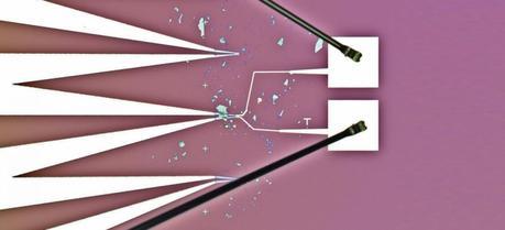
 Microscope photograph of WSe2-samples, connected to electrodes. (Credit: TU Wien)
Researchers at the Vienna University of Technology have succeeded for the first time in creating a diode made of tungsten diselenide. Experiments show that this material may be used to create ultrathin flexible solar cells. Even flexible displays could become possible.
At least since the Nobel Prize in physics was awarded in 2010 for creating graphene, the “two dimensional crystals” made of carbon atoms have been regarded as one of the most promising materials in electronics. In 2013, graphene research was chosen by the EU as a flagship-project, with a funding of one billion euros. Graphene can sustain extreme mechanical strain and it has great opto-electronic properties. With graphene as a light detector, optical signals can be transformed into electric pulses on extremely short timescales.

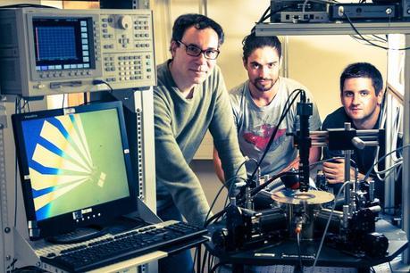
Left to right: Thomas Müller, Marco Furchi, Andreas Pospischil. (Credit: TU Wien)
For one very similar application, however, graphene is not well suited for building solar cells. “The electronic states in graphene are not very practical for creating photovoltaics”, says Thomas Mueller. Therefore, he and his team started to look for other materials, which, similarly to graphene, can arranged in ultrathin layers, but have even better electronic properties.
The material of choice was tungsten diselenide: It consists of one layer of tungsten atoms, which are connected by selenium atoms above and below the tungsten plane. The material absorbs light, much like graphene, but in tungsten diselenide, this light can be used to create electrical power.
The layer is so thin that 95% of the light just passes through—but a tenth of the remaining five percent, which are absorbed by the material, are converted into electrical power. Therefore, the internal efficiency is quite high. A larger portion of the incident light can be used if several of the ultrathin layers are stacked on top of each other—but sometimes the high transparency can be a useful side effect. “We are envisioning solar cell layers on glass facades, which let part of the light into the building while at the same time creating electricity”, says Thomas Mueller.
Today, standard solar cells are mostly made of silicon, they are rather bulky and inflexible. Organic materials are also used for opto-electronic applications, but they age rather quickly. “A big advantage of two-dimensional structures of single atomic layers is their crystallinity. Crystal structures lend stability”, says Thomas Mueller.
The results of the experiments at the Vienna University of Technology have now been published in Nature Nanotechnology (see footnote). The research field is extremely competitive: in the same issue of the journal, two more papers are published, in which very similar results are shown. Researchers at the MIT (Cambridge, USA) and at the University of Washington (Seattle, USA) have also discovered the great advantages of tungsten diselenide. There seems to be little doubt that this material will soon play an important role in materials science all over the world, much like graphene has in the last couple of years.
Pospischil, A., Furchi, M., & Mueller, T. (2014). Solar-energy conversion and light emission in an atomic monolayer p–n diode Nature Nanotechnology DOI: 10.1038/nnano.2014.14
