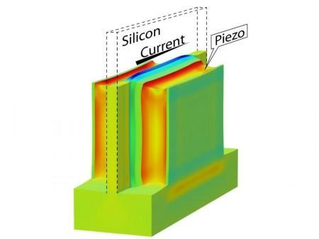
 The electrical current passing through a transistor is conducted by a slice of silicon. In the
 new transistor, this is sandwiched between layers of piezoelectric material. As this material
(shown in red) expands, the silicon (shown in blue) is compressed. (Credit: See citation at
the end of this article)
Tom van Hemert and Ray Hueting of the University of Twente’s MESA+ Institute for Nanotechnology have found a way to “plug” leakage current in transistors by “squeezing” the transistor with a piezoelectric material. This cuts the unnecessary energy losses, potentially increasing the battery life of portable electronic devices.
If silicon is squeezed, this affects the freedom of movement of the electrons in this material. This can promote or restrict the flow of electrical current. This effect can be compared to a garden hose that is constricted so that that very little water comes out. Only with silicon, it’s the other way around: When the material is compressed, the flow of electrons in silicon actually increases.
In modern microchips, every single transistor is continuously exposed to enormous pressures of up to 10,000 atmospheres. This pressure is sealed in during the manufacturing process, by surrounding the transistors with compressive materials. While this boosts the chip’s processing speed, the leakage current also increases. The use of piezoelectric material (that expands or contracts when an electrical charge is applied to it) means that the transistors are only put under pressure when this is necessary. This can generate considerable savings in terms of energy consumption.
The underlying concept was originally developed by Ray Hueting. In order to turn this into reality, Tom van Hemert had to find a way of linking theories of mechanical deformation with quantum-mechanical formulas describing the electrical behavior of transistors. The calculations indicate that “garden hose transistors” are much better than conventional transistors at switching from off to on. According to the classical theoretical limit, a charge of at least 60 millivolts is needed to make a transistor conduct ten times more electricity. The piezoelectric transistor uses just 50 millivolts. As a result, either the leakage current can be reduced, or more current can be carried in the on-state. Either way, this will boost the performance of modern microchips, while cutting their energy consumption.
Piezoelectricity is the electric charge that accumulates in certain solid materials in response to applied mechanical stress. The piezoelectric effect is a reversible process: For example, lead zirconate titanate crystals will generate measurable piezoelectricity when their static structure is deformed by about 0.1% of the original dimension. Conversely, those same crystals will change about 0.1% of their static dimension when an external electric field is applied to the material. van Hemert T., & Hueting R.J.E. (2013). Piezoelectric Strain Modulation in FETs IEEE Transactions on Electron Devices, 60 (10), 3265-3270 DOI: 10.1109/TED.2013.2274817
