 (Credit: Flickr @ James Smile Click! http://www.flickr.com/photos/smileclick/)
Research teams at the Helmholtz-Zentrum Berlin for Materials and Energy (HZB) and at the University of Limerick, Ireland, have discovered a novel solid state reaction that can create a kesterite thin film solar cell absorber from a carpet of nanorods within a few seconds.
The reaction lets kesterite grains grow within a few seconds and at relatively low temperatures. For this, the researchers use a transition from a metastable wurtzite compound in the form of nanorods to the more stable kesterite compound. The scientists can observe this process in real-time when heating the sample: in a few seconds Kesterite grains are formed. The size of the grains was found to depend on the heating rate. With fast heating, the scientists succeeded in producing a Kesterite thin film with near micrometer-sized crystal grains, which could be used in thin film solar cells. These findings have now been published in the journal Nature Communications (see footnote).
Kesterite is a sulfide mineral with a formula Cu2(Zn,Fe)SnS4. In its lattice structure, zinc and iron atoms share the same lattice sites. Kesterite is the Zn-rich variety whereas the Zn-poor form is called ferrokesterite or stannite. Owing to their similarity, kesterite is sometimes called isostannite. The synthetic form of kesterite is abbreviated as CZTS (from copper zinc tin sulfide). The name kesterite is sometimes extended to include this synthetic material and also CZTSe, which contains selenium instead of sulfur.
CZTS is a quaternary semiconducting compound which has received increasing interest since the late 2000s for applications in solar cells. CZTS solar cells with efficiency up to 2.3% were reported in 1997, as well as CZTSe devices. Recent material improvements for CZTS have increased efficiency to 12.6% in laboratory cells, but more work is needed for their commercialization.

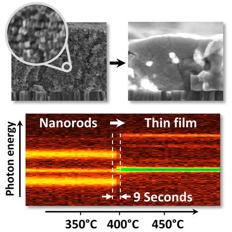
The transformation from a layer of closely packed nanorods (top left) to a polycrystalline semiconductor thin film (top right) can be observed in by in-situ X-ray diffraction in real time. The intensities of the diffraction signals are color coded in the image at the bottom. A detailed analysis of the signals reveals that the transformation of the nanorods into kesterite crystals takes only 9 to 18 seconds. (Credit: R. Mainz / A. Singh). Click to enlarge.
Chemists at the University of Limerick have fabricated films of highly ordered wurtzite nanorods, which have exactly the same composition as kesterite Cu2ZnSnS4. With the help of real-time X-ray diffraction, HZB physicists around Roland Mainz and Thomas Unold could now observe how a phase transition from the metastable wurtzite phase to the stable kesterite phase leads to a rapid formation of a thin film with large kesterite grains.
“It is interesting to see that the complete formation of the kesterite film is so fast”, says Mainz. And the faster the samples are heated up, the larger the grains grow. Mainz explains that at low heating rate, the transition from wurtzite to kesterite starts at lower temperature at which many small grains form—instead of a few larger grains. Additionally, more defects are formed at lower temperatures. During fast heating, the transition takes place at higher temperature at which grains with less defects form.
Moreover, the comparison of the time-resolved evolution of the phase transition during slow and during fast heating shows that not only the grain growth is triggered by the phase transition, but also the phase transition is additionally accelerated by the grain growth. The HZB physicists have developed a model which can explain these findings. By means of numerical model calculations, they demonstrated the accordance of the model with the measured data.
The work points towards a new pathway for the fabrication of thin microcrystalline semiconductor films without the need of expensive vacuum technology. Cu2ZnSnS4-based kesterite semiconductors have gained increasing attention in the past, since they are a promising alternative for the Cu(In,Ga)Se2 chalcopyrite solar cells which already achieved efficiencies above 20%. Kesterite has similar physical properties as the chalcopyrite semiconductors, but consists only of elements which are abundantly present in the earth crust. The new procedure could also be interesting for the fabrication of micro- and nanostructured photoelectric devices as well as for semiconductor layers consisting of other materials, says Mainz. “But we continue to focus on kesterites, because this is a really exciting topic at the moment.”
Mainz R., Singh A., Levcenko S., Klaus M., Genzel C., Ryan K.M., & Unold T. (2014). Phase-transition-driven growth of compound semiconductor crystals from ordered metastable nanorods. Nature Communications, 5 PMID: 24448477
