 Silicon carbide (SiC) monocrystal from the LMGP (Minatec) lab in Grenoble, France. (Credit: David Monniaux http://commons.wikimedia.org/wiki/User:David.Monniaux)
Scientists at the University of Tokyo have developed a novel dielectric film growth technique which improves the performance of SiC power devices.
High performance power devices, which are used for high current, high voltage and high frequency applications, offer the potential for large energy saving. In particular, silicon carbide (SiC) devices offer the potential for lower energy loss than conventional silicon devices. However, SiC transistors suffer from high resistance and low reliability, mainly due to defects formed at the interface between SiC gate dielectric film. Such defects, caused by impurities and atomic excess or deficiency at the interface, need to be reduced to improve the performance.
SEE ALSO: Topological Insulators Could Power Memory Devices

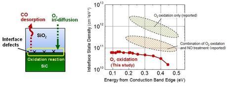
(Left) Schematic of oxidation of SiC/SiO2 interface. The desorption of byproduct carbon as carbon monoxide is an effective way to reduce interface defect formation. (Right) Interface state density of 4H-SiC/SiO2 observed in this study, compared with previously reported typical values (hatched areas). The horizontal axis shows the energy levels of defect states referred to the conduction band edge of SiC. (Credit: Koji Kita)
The research group of Associate Professor Koji Kita at the University of Tokyo Graduate School of Engineering, found that the density of interface defects is significantly reduced by employing reaction conditions where the byproduct carbon is ejected as carbon monoxide when creating the gate dielectric film. The group achieved the lowest defect density in a MOS (metal-oxide-semiconductor) test structure employing these conditions.
This technique provides a high quality SiC interface without any extra processes such as addition of nitrogen-containing gases, assuring the easy industrial application of this method. This technique is expected to improve the performance and accelerate the spread of SiC power devices, contributing to energy saving in a variety of applications, including electric power transmission, electric vehicles, and factory machines.
Kikuchi, R., & Kita, K. (2014). Fabrication of SiO2/4H-SiC (0001) interface with nearly ideal capacitance-voltage characteristics by thermal oxidation Applied Physics Letters, 105 (3) DOI: 10.1063/1.4891166
