 (Credit: Flickr @ Jørgen Schyberg http://www.flickr.com/photos/mrjorgen/)
A team of scientists at the Helmholtz-Zentrum Berlin for Materials and Energy have developed a way to produce chalcopyrite solar cells without cadmium-based buffer layer. A single layer takes on the job of what used to be two layers, doing away with the wet chemical process. Despite a much simplified production method, efficiencies of greater than 18 percent are well within reach.
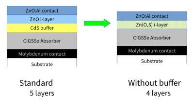
A chalcopyrite thin film solar cell is normally made up of five layers, each of which performs a unique job. Every single one of these layers has been optimized over many years to ensure chalcopyrite solar cells now reach very high efficiencies of greater than 20 percent. At the same time, from an economic perspective, reducing the number of steps of production and uniting the functions of separate layers into one single layer is of great interest.
“One layer we could happily do without is the cadmium sulfide based buffer layer,” explains Dr. Reiner Klenk of the HZB Institute for Heterogeneous Material Systems. The reason being that a wet chemical bath deposition is used to produce this layer, involving chemicals that are considered problematic and because the process is difficult to integrate in the chain of otherwise dry physical methods of deposition.

A chalcopyrite thin film solar cell is normally made up of five layers (left). HZB-scientists have managed to reduce the number of steps of production and uniting the functionalities of two layers into one single layer which does not contain cadmium. (Credit: R. Klenk / HZB)
The HZB researchers have now managed to modify the i- zinc oxide layer, which sits on top of the buffer layer, in such a way as to have it take on the job of buffer. In a process known as sputtering, the zinc oxide layer is produced by vaporizing a zinc oxide target as cathode using plasma and depositing it onto the sample. However, whether sputtering it directly onto the chalcopyrite absorber layer would also work was unclear. Because the chalcopyrite layer is sensitive, one of the buffer layer’s functions was supposed to be protecting this sensitive layer from energetic particle bombardment during sputtering. In fact, prior work has consistently shown a loss of efficiency.
“The breakthrough came when we opted for a zinc (Zn) oxygen (O) sulfur (S) compound as i-layer,” explains Alexander Steigert. The scientists first sputtered a ZnS cathode in gas mixtures containing different parts oxygen in a facility directly coupled to a surface analysis system (“CISSY”). Layer properties were measured as a function of the S/(S+O) ratio and initial solar cells were produced that ended up working rather well. As soon as the optimal ratio had been determined, a properly mixed target was built in. Says Klenk: “We were able to show that this actually works. For production, you would really only need to replace the ZnO target with a ZnO/ZnS target at a set mix ratio, which would allow you to do without any preceding deposition of a dedicated buffer layer. Meaning we would have realized a dry, Cd-free, in-line process without a major investment.”
In the lab, this now works without having to compromise efficiency. The HZB researchers were able to get up to 18.3 per cent, a number that was confirmed by measurements taken at the renowned ISE Fraunhofer Institute in Freiburg, Germany. Compared with other approaches to producing cadmium-free solar cells, with this process, pretreating the surface or following up with a temperature treatment have become obsolete. “There is even still some wiggle room for further increasing the standard module’s efficiency,” says Klenk.
“In addition to scientific interest, the notion that this technology would be much simpler for industry was yet another motivating factor. We successfully tested our technology using industrial substrates. As part of the NeuMaS Project (Manz, Bosch CISTech), we are evaluating multiple approaches for Cd-free modules in order to determine which technology is best to use during production,” explains Prof. Dr. Martha Lux-Steiner, head of the Institute for Heterogeneous Material Systems.
This way, the zinc oxide sulfide layer could be sputtered during industrial production and the next layer added with an aluminum-doped zinc oxide target, doing away with the conventional wet chemical protocol. “Not only were we able to show that this actually works, we also confirmed that these cells hold top efficiency potential,” stresses Christian Kaufmann, who is leading a group that is investigating high quality chalcopyrite layers.
At this point, Klenk’s group is retrofitting an existing sputtering facility to allow for homogeneous coating of large surfaces. “This would allow us to produce CIGSe modules of 30 by 30 centimeters and we could also test their long-term stability, as, after all, in terms of perspective, it’s all about this new environmentally-friendly process being interesting to industry and capable of yielding top efficiency, stable solar modules,” says Klenk.
Klenk, R., Steigert, A., Rissom, T., Greiner, D., Kaufmann, C. A., Unold, T. and Lux-Steiner, M. Ch. (2013). Junction formation by Zn(O,S) sputtering yields CIGSe-based cells with efficiencies exceeding 18% Progress in Photovoltaics: Research and Applications DOI: 10.1002/pip.2445
